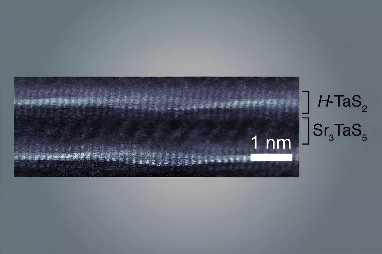
Recent advancements by MIT physicists and their collaborators have unveiled a novel material that showcases both superconducting and metallic properties, a development rooted in the extraordinary design of its atomic structure. This material features intricately wavy layers of atoms, each merely a billionth of a meter thick, which stack to form a macroscopic sample. The size of this sample is particularly significant; it allows researchers to more readily investigate its quantum behavior—interactions occurring at the atomic level—thus leading to a better understanding of the material’s unique characteristics.
The implications of this work, detailed in the prestigious journal *Nature*, extend beyond the synthesis of a single new material. The process behind the material’s creation stems from a rational design approach, which is fundamentally grounded in the researchers’ deep knowledge of materials science and chemistry within the realm of superconductors. This foundational insight instills confidence among physicists that they will be able to forge even more materials that exhibit extraordinary properties. In this respect, the innovative approach taken by the team indicates a significant step forward, not simply in terms of characterizing materials but in their cultivation as well.
Central to the material’s uniqueness is its exquisite atomic architecture. Unlike traditional materials, where the atomic structure is uniform and predictable, this new material is characterized by a remarkable consistency of wavy atomic layers throughout an entire crystal. Professor Joseph Checkelsky, a senior investigator in the project, emphasized that these materials transcend typical definitions of a crystal. The challenge lies in observing and comprehending the novel physical phenomena that may arise from such non-conventional structures.
As the scientific community continues to delve deeper into the world of two-dimensional materials—those consisting of just one or a few atomic layers—there is a growing realization that their intricate manipulation can yield unique properties. One fascinating method of alteration, twisting the layers at microscopic angles to create moiré superlattices, has proven to foster new phenomena such as unconventional magnetism and superconductivity. However, creating such moiré materials has traditionally been a labor-intensive and cumbersome task due to their inherently small dimensions.
The research group led by Checkelsky aims to simplify this process by designing materials that can be synthesized through relatively straightforward methods. As highlighted by Aravind Devarakonda, who took the lead on the study, the synthesis involves mixing various powders and exposing them to high temperatures in a furnace, resulting in the spontaneous formation of macroscopic crystals. This streamlined approach not only enhances the scalability of material production but also makes exploration of their atomic-scale interactions much more feasible.
Digging into the details of the new material, its layered structure can be likened to a multi-tiered cake, composed of alternating thin layers of tantalum and sulfur alongside a “spacer” layer formed from strontium and tantalum. The repetition of these layers over thousands forms crystal structures that are unprecedented in their perfection. The researchers posit that the wavy formations arise from discrepancies in the crystal lattice size and structure of each layer. Analogous to fitting a larger sheet of paper on a smaller one, the layers must buckle to create a cohesive structure, resulting in a captivating array of minuscule waves that actively contribute to the material’s intriguing physical properties.
One such property is superconductivity—the phenomenon where electrons traverse a material without resistance. Within this new compound, these electrons are influenced by the structural fluctuations imparted by the wavy pattern of the layers. This variability results in varying levels of superconductivity based on the local wave structure, meaning some areas may allow electrons to flow freely while others may experience resistance.
Moreover, these materials also exhibit distinct metallic characteristics. Electrons find it easier to navigate the troughs of the wavy structures than to climb over the peaks, thereby creating directional flow properties for electrical conduction. This directional advantage significantly alters the material’s behavior, leading to designer properties that were previously unimagined.
The ramifications of this research extend far beyond the mere creation of a new superconductor. Devarakonda’s remarks about the discovery mark the beginning of an entirely new category of materials. As the team prepares to venture further into this uncharted territory, the potential for unexpected outcomes and revolutionary applications arises.
The collaboration includes not only physicists but also experts from various institutions, signifying a cross-disciplinary effort that bolsters the comprehensive understanding of these complex materials. As they stand atop the foundation laid by predecessors in the field, this team is poised to expand the horizons of material sciences, forging pathways for future innovations and applications.
MIT’s groundbreaking work in synthesizing a new class of wavy materials holds the promise of not just advancing theoretical understanding, but also fostering real-world applications in technology and engineering, likely altering the landscape of material science as we know it.

